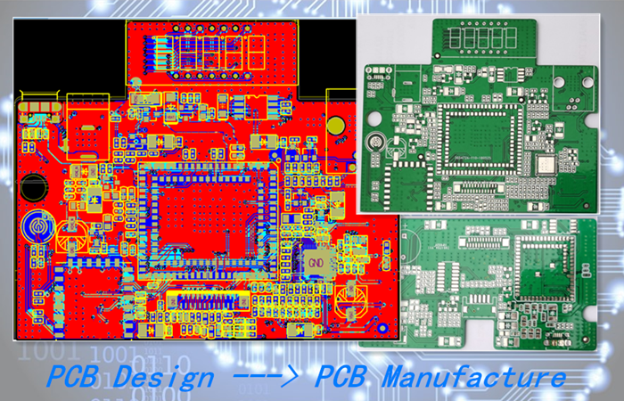
PCB Design
PCB is our main business, providing our customers with complete PCB solutions. We have a professional technical team, providing customers with comprehensive technical support in PCB design services.
We have a good technical team with many experienced engineers, 5% revenue spend on R&D leading innovation of PCB technology. We offer customized end-to-end solution from PCB design to manufacture.
Professional Team
We have a professional PCB design team, and all PCB engineers have more than 5 years experience in PCB design
One-Stop PCB solution
WINTO provides one-stop solution from PCB design to manufacture. The markets we serve include telecommunications and networking, industry, automotive, energy, security, healthcare, etc.

PROJECT PRESENTATIONS
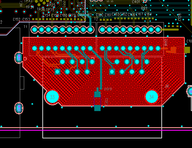
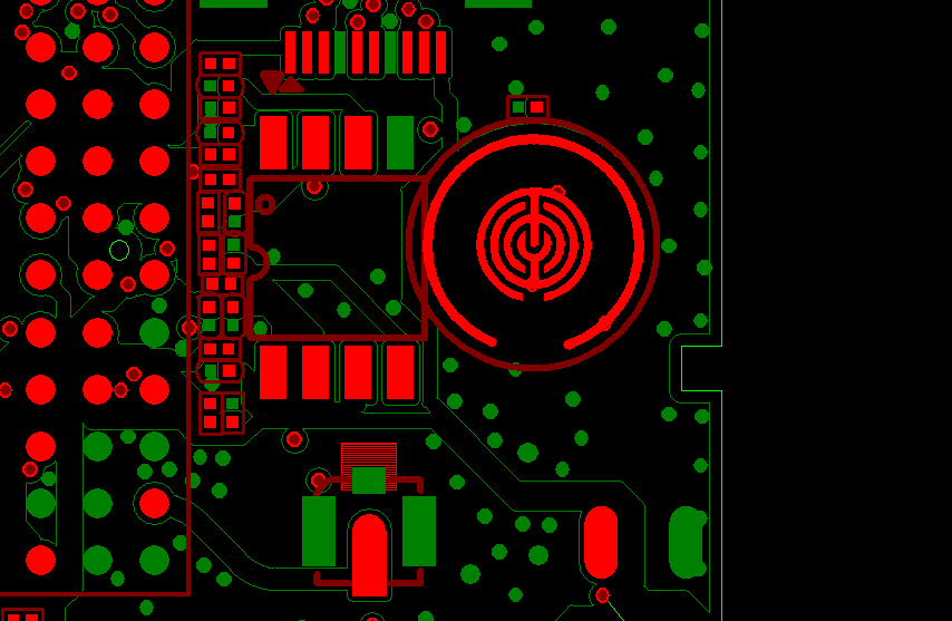
Project 1st: POS PCB Design
This project is a main PCB for POS (payment terminal product), designed to meet PCI certification requirements. Our customer entrusts us to do PCB design, prototype production and mass production. Our design successfully passed customer verification and entered the mass production stage.
| Product Categories | POS | PCB Layer | 6L |
|---|---|---|---|
| Differential Impedance | 100 Ohm | Min.line width/space | 0.1mm/4mil |
| Minimum hole diameter | 0.4mm | Surface finishing |
immersion gold+gold finger |

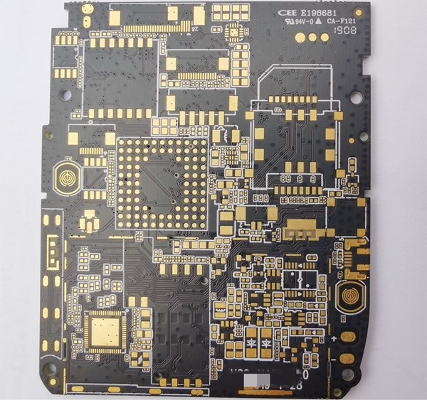
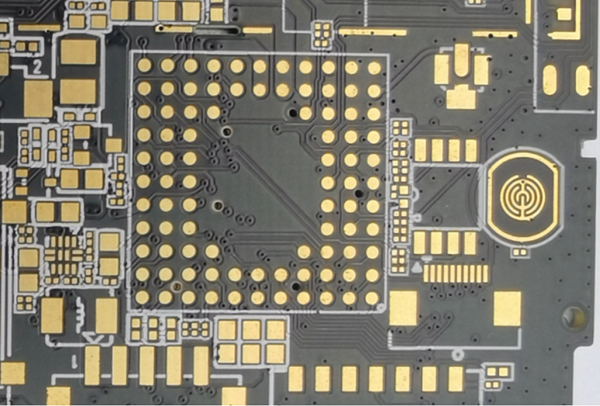
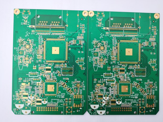
Project 2nd: Industrial Communication Device (RTL9607C)
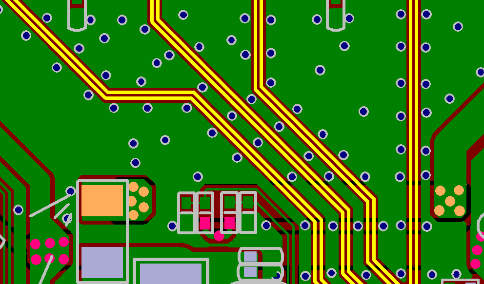
This project is to design a fiber optic communication product (GPON). We design PCBs, make samples and supply PCBs in batches for customers. The CPU is Realtek's RTL9607 in this case. The key points of the design are high-speed signal processing, radiation and electrostatic protection, and impedance control. Our engineers provide customers with professional design solutions, which are recognized by customers
| Product Categories | GPON | PCB Thickness/ Layer | 1.6mm/4L |
|---|---|---|---|
| Differential Impedance | 100 Ohm | Min.line width/space | 0.075mm/3mil |
| Minimum hole diameter | 0.3mm | Surface finishing |
immersion gold |